Download PDF of this White Paper ![]()
By Terry Stratoudakis – Wall Street FPGA, LLC – New York City – March 2011
Abstract
This paper presents a Hardware Accelerated FIX Order Cancel System. The open source FIX Engine, QuickFIX is accelerated using Field Programmable Gate Array (FPGA) technology. The acceleration is performed by an FPGA based network card which is optimized for QuickFIX. FIX 4.2 Order Cancel messages are generated entirely inside the FPGA. The latency from the Order Cancel trigger to when the first byte is on the wire is 314 nanoseconds. The latency from the Order Cancel trigger to when the first FIX Order Cancel message is entirely on the wire is 1,874 nanoseconds.
Introduction
The majority of trading is increasingly done electronically using computers; see Figure 1. Peak trading periods provide among the best trading opportunities for profits but also present the largest risk for potential losses. During peak trading periods, market data that trading systems must consume and process surges to the point where trading systems slow down and become ineffective.
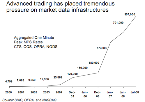
Figure 1 – Aggregate One Minute Peak Messages Per Second
High Frequency Trading (HFT) is impacting market dynamics and generated interesting debates. For some, HFT is a relative term. What is called HFT today may be the common form of trading in the future. And whether or not a firm engages in HFT, they will certainly need to protect their assets from events such as the “Flash Crash” of May 6, 2010. It is possible that a trading firm using an FPGA based Order Cancel system could have exited the market faster than any other trading firm – thereby reducing losses on days such as this one; see Figure 2 below.

Figure 2 – Dow Jones Industrial Average on May 6, 2010 (“Flash Crash”)
FIX Protocol
Financial firms communicate market and trade data via messaging standards such as the FIX protocol. The Financial Information eXchange (FIX) Protocol is a messaging standard for the real-time electronic exchange of securities transactions. The FIX standard is managed by FIX Protocol Limited (FPL), an international non-profit standards body with members from all aspects of the financial services industry.
Software known as FIX Engines are used to process and generate FIX messages. QuickFIX is the de facto open source FIX Engine. QuickFIX as well as commercial “closed source” FIX Engines are used by financial firms.
Financial firms are turning to High Performance Computing (HPC) technology to provide that extra advantage over their competitors. Every level of software is optimized, and in recent years, firms are optimizing the hardware of their trading systems through the use of reconfigurable hardware.
FPGAs: Reconfigurable Hardware
Reconfigurable hardware such as Field Programmable Gate Array (FPGA) technology is used to optimize trading systems at the network level. FPGAs can aid in the generation and processing of network data thereby offloading certain tasks from the software of a system. The most common usage of FPGAs in finance is Market Data Handling. FPGAs can have up to 1000 cores for processing data in parallel and do not have the jitter introduced by operating systems and instruction fetching.
An FPGA is programmed using a Hardware Description Language (HDL) such as Verilog or VHDL. Not all algorithms can be implemented on an FPGA. This is partly due to the nature of FPGAs as a technology and also due to the low level aspect of HDL. HDL requires more knowledge of the target hardware than traditional programming such as C or C++. HDL coding can result in development times of 3 to 5 times more if the algorithm can even be implemented on an FPGA. These languages are difficult to learn and result in very lengthy source code files that often accomplish very little with a lot of effort. For example, the VHDL code for calculating the square root of a number can take anywhere from 117 lines to 396 lines of code.
The FIX Protocol is string based, lending itself to large benefits from an FPGA. String functions are among the least efficient in a CPU.
Technology Platform
The technologies used in this system are PXI, FlexRIO, and LabVIEW FPGA.
PXI
PXI (PCI eXtensions for Instrumentation) is an open and standardized computer bus using the CompactPCI form factor. PXI is based on the PCI bus with integrated timing and synchronization that is used to route clocks and triggers internally. PXI was developed in 1997 and launched in 1998. Today, PXI is governed by the PXI Systems Alliance (PXISA), a group of more than 70 companies chartered to promote the PXI standard, ensure interoperability, and maintain the PXI specification. PXISA is also responsible for the PXI Express bus which is based on the PCI Express computer bus found in newer computers.
PXI systems are composed of three basic components — chassis, controller, and peripheral modules. For example, an 18 slot 19 inch rack-mountable chassis holds one controller and 17 single slot modules. The controller contains laptop sized components for compactness and can run Windows, Linux, and various real-time operating systems. There are 3U and 6U modules.
Since PXI is based on standard PC technologies such as Windows and the PCI bus, integrating a PXI system to these systems is similar to integrating these systems with a PC. PXI also supports a broad range of Compact PCI products as they are both based on the same form factor.
The PXI bus combines the high-speed PCI bus with timing and synchronization. The PXI trigger bus consists of 8 shared trigger bus lines, a low-skew star trigger, and a common 10 MHz system reference clock. Using these synchronization features, one can pass trigger, clock, and other signals between PXI modules to make the accurate, high-performance measurements.
FlexRIO
FlexRIO is a PXI and PXI Express based reconfigurable hardware platform developed by National Instruments. It features two parts: FlexRIO field-programmable gate array (FPGA) modules and FlexRIO adapter modules. Together, they form a high-performance, reconfigurable hardware system programmable with LabVIEW FPGA software and without Hardware Description Language (HDL) design knowledge.
NI FlexRIO FPGA Modules
FlexRIO FPGA modules utilize a Virtex-5 FPGA with up to 512 MB of onboard DDR2 DRAM. FlexRIO FPGA modules come in PXI and PXI Express formats and interface to FlexRIO adapter modules that provide I/O to the FPGA. PXI FlexRIO modules have three (3) DMA channels for high-speed data streaming while the PXI Express FlexRIO modules have sixteen (16) DMA channels. See Figure 3.
The adapter module interface consists of 132 lines of general-purpose digital I/O directly connected to FPGA pins, in addition to the power, clocking, and supplementary circuitry necessary to define the interface. These 132 lines can be configured for single-ended operation at rates of up to 400 Mbits/s and differential operation at rates of up to 1 Gbit/s for a maximum I/O bandwidth of 66 Gbits/s (8.25 GB/s). All lines are routed with controlled-impedance, matched-length traces, and the differential pairs are routed together.
Peer-to-Peer Data Streaming is unique to PXI Express NI FlexRIO FPGA modules. This allows banks of up to four (4) PXI Express NI FlexRIO FPGA cards to deterministically communicate with each other. They are capable of streaming data between modules at rates above 800 MB/s and latencies of no more than 10 microseconds as data is not routed through the host chipset. Up to 16 such streams are supported, simplifying complex multi-FPGA communication schemes without taxing host CPU resources.
FlexRIO cards have RTSI, or Real Time Signal Integration, which enables cards to be synchronized using the PXI bus. RTSI enabled devices can communicate directly over a low latency electrical connection.
NI FlexRIO FPGA modules are accessible by Windows, Linux, PharLap, and VxWorks Operating Systems via the NI RIO drivers; version 3.5.1 of the RIO drivers were used for this application.

Figure 3 – FlexRIO FPGA Module
FlexRIO Adapter Modules
FlexRIO Adapter modules from National Instruments and third parties interface with FlexRIO FPGA modules through a card-edge connector that routes the necessary FPGA signals to the adapter module. Custom adapter modules can be developed with the NI FlexRIO Adapter Module Development Kit (MDK).
The FlexRIO Adapter Module Development Kit (MDK) can be used to build custom I/O to meet exact application needs. The FlexRIO card edge connector offers direct access to the raw digital I/O pins of the FPGA. Each pin is capable of low-voltage differential signaling (LVDS) rates up to 1 Gb/s and single-ended rates up to 400 Mb/s. The adapter modules are interchangeable and define the I/O available in the LabVIEW FPGA programming environment.
In this paper the Prevas Mimas Gigabit Ethernet Adapter is used, see Figure 4 below.
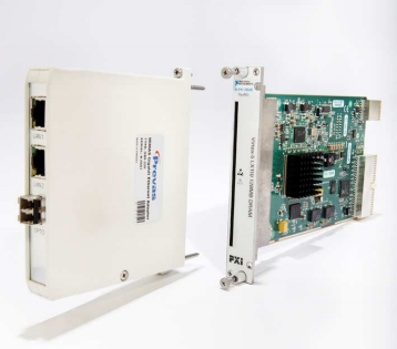
Figure 4 – Prevas Mimas connected to NI FlexRIO Module
LabVIEW FPGA
FPGAs are field programmable which saves on development and modification costs. Prior to FPGAs, custom logic required schematic design which led to Register Level Transfer (RTL). RTL which was replaced by Verilog and VHDL. Increased FPGA capacity requires a higher level of abstraction. In the past decade, industry has developed High Level HDLs. This allows for more complex algorithms to be implemented in a more timely fashion.
National Instruments’ LabVIEW FPGA platform provides a graphical approach to developing logic for an FPGA. Complex financial algorithms can be programmed onto FPGAs without in-depth knowledge of digital design or complex Electronic Design Automation (EDA) tools. LabVIEW is distinctly suited for FPGA programming because it provides an intuitive depiction of the inherent parallelism that FPGAs provide. Using a high level, graphical development environment (see Figure 5) of LabVIEW FPGA reduces development time without compromising the performance gains of using an FPGA.
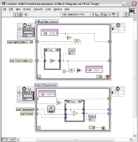
Figure 5 – LabVIEW FPGA sample Block Diagram
Under the hood, the LabVIEW FPGA module uses code generation techniques to synthesize the graphical development environment to FPGA hardware which ultimately runs the FPGA synthesis tools. The single-cycle timed loops (SCTL) in LabVIEW FPGA provide a level of determinism guaranteed to execute within a specified time period of at least 40 MHz. In this paper, a SCTL running at 125 MHz was used.
Custom hardware can be used to create unique timing and triggering routines, ultrahigh-speed control, interfacing to digital protocols and applications requiring high-speed hardware reliability and tight determinism. In this paper, LabVIEW FPGA is used to create a protocol aware hardware based system.
Scenario
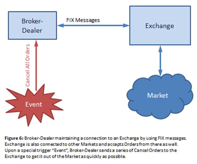
A broker-dealer is connected to an exchange. The trade messages between the broker-dealer and the exchange use the FIX protocol format. The broker-dealer submits orders which the exchange seeks to match. All orders from the broker-dealer are open until a matching order enters the exchange. Matched orders are sent back to the broker-dealer as executed. At some point, the broker-dealer detects an “event” resulting in its need to cancel all open orders. It is assumed that the detected event is one which will cause many other broker-dealers to wish to cancel their open orders at the same time, so time would be of the essence and those who cancel first will reduce their potential losses. See Figure 6 below.
Implementation
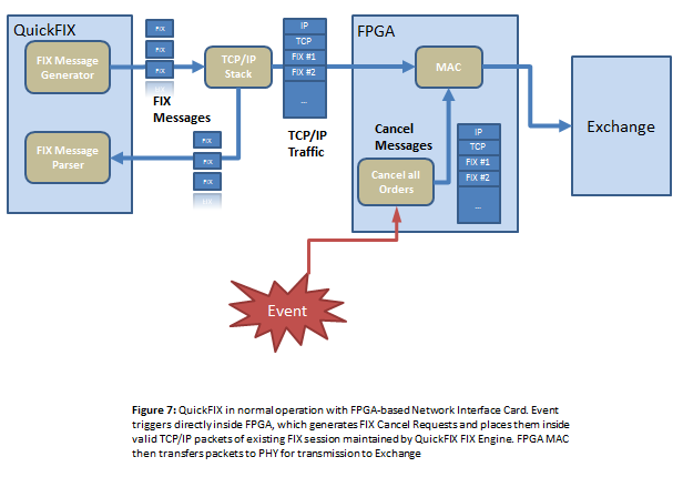
This was implemented using two computers connected directly via a cross over Ethernet cable. They communicate using FIX 4.2 running over TCP/IP at 1 Gigabit/second. Both computers are running Microsoft Windows XP on Intel x86 CPUs. One computer represents the Broker-Dealer, and the other the Exchange. The Broker-Dealer sends to the Exchange several buy or sell orders such that they do not execute. Upon detection of a trigger, the Broker-Dealer sends FIX Order Cancel messages for all open orders. See Figure 7.
Broker-Dealer Computer
The Broker-Dealer computer is comprised of a computer connected to a NI PXI-1033 5-Slot PXI Chassis with Integrated MXI-Express Controller. Two PXI cards are plugged into the PXI chassis; a FlexRIO PXI-7953 FPGA card with a Xilinx Virtex-5 LX85 FPGA and a NI PXI-6070E DAQ card. The FlexRIO card has a Prevas Mimas Gigabit Ethernet Adapter which has two RJ-45 connectors. The FlexRIO and Prevas Mimas adapter combine to function as the Network Interface Card (NIC) of the Broker-Dealer computer. All network traffic goes through the FlexRIO card and one of the ports of the Prevas Mimas Dual Gigabit adapter (the other port is unused for this application).
The Prevas Mimas adapter has a ‘PHY’ chip which converts inbound electrical signals on an RJ-45 cable to Ethernet Frames and vice versa. The Ethernet frames come into the Xilinx Virtex-5 LX85 FPGA in the form of bytes (U8).
Under normal conditions, the FlexRIO FPGA card allows the layer 2 Ethernet frame data to go out via the Prevas Mimas adapter and in by passing it into the PXI bus so that it is accessible by programs that interface to the NI RIO drivers.
QuickFIX normally interfaces with Winsock functions which interface with Windows’ closed source TCP/IP stack. Being closed source, it cannot interface to the RIO drivers and therefore lwip, an open source TCP/IP stack, was selected instead. All of QuickFIX’s calls to Winsock were modified to call the lwip TCP/IP stack which in turn was modified to interface with the RIO drivers.
The NI PXI-6070E Data Acquisition card was used to receive and transfer the Cancel Orders trigger. One of the PXI RTSI lines was used to make a direct electrical connection between this and the FlexRIO FPGA card. An external button was connected to one of the DAQ card’s digital inputs such that when pressed, a digital signal would be read by the FPGA. This is read purely in hardware with no interaction by the computer or the software.
Exchange Computer
The Exchange computer is comprised of another computer running an unmodified version of QuickFIX running in server mode. Network interfacing is done via the native Gigabit Ethernet port. Its function is to hold an order open until either a matching one arrives, or the order is cancelled.
Results
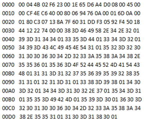
Several non-matching orders are entered into the Broker-Dealer’s QuickFIX program. It sends them to the Exchange computer which holds them as open orders. The Broker-Dealer’s QuickFIX program maintains a list of its own open orders. Whenever any aspect of the open orders changes on the Broker-Dealer, the FPGA receives a copy of the cancellation information for each open order. Below is a sample FIX 4.2 Order Single (tag 35=D) message in offset hex and then the readable characters only.

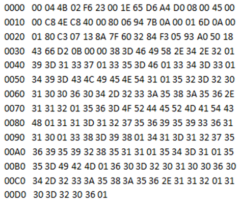
Below is a sample FIX 4.2 ORDER CANCEL REQUEST (tag 35=F) message in offset hex and then the readable characters only.

Pressing the button connected to the PXI-6070E DAQ card generates a Cancel Orders trigger, which causes the FPGA to generate one FIX Order Cancel message for each of the open orders. The FIX message(s) are then injected into the live TCP session that already exists between the Broker-Dealer and Exchange machines. The Exchange computer receives the FIX Order Cancel messages, not realizing that those messages were created by the FPGA [and not by QuickFIX on the Broker-Dealer computer] it cancels all orders referenced as if the Broker-Dealer instructed it to do so.
For all normal FIX traffic, the QuickFIX application handles the creation of each FIX message, while the software TCP/IP stack handles the creation of TCP segments and IP packets. In the situation where a Trigger event has just occurred, the FPGA handles all the tasks of QuickFIX and the TCP/IP software by generating the FIX message(s), TCP segment(s), and IP packet(s). As the final payload is being transferred to the PHY, the Ethernet frame and CRC is also calculated by the FPGA.
Conclusion
Field Programmable Gate Array (FPGA) technology has been established for Market Data and is now finding applications such as trade message generation. Trade volume and data increases are outpacing trading system technology. Financial firms seek to optimize every aspect of the trading system. Until recently, software has been the focus of optimizations.
Hardware optimization provides the lure of creating “the world’s fastest and most deterministic trading system” and is the last frontier of customization. This is not without cost as a completely customized hardware optimized system can easily become a zero-sum game.
Using off the shelf FPGA boards and a High Level Hardware Description Language (HDL) such as LabVIEW FPGA, one can develop hardware accelerated trading system with managed risk and costs. PXI is a platform for FPGA based solutions that can integrate IEEE-1588v2 (2008) timestamps from a GPS time source and latency measurements. PXI Express FPGA boards can efficiently communicate amongst themselves [without the host CPU] using Peer-to-Peer Data Streaming to provide multi-FPGA trading systems.
Financial firms can now optimize both software and hardware of their trading systems to provide further differentiation and increase their competitiveness.
About Wall Street FPGA, LLC
Wall Street FPGA, LLC (www.WallStreetFPGA.com) is a New York City-based boutique financial technology firm that delivers hardware accelerated, low latency, high throughput financial trading and analytics solutions. Wall Street FPGA, LLC combines knowledge of capital markets and disruptive technology. For more information and to schedule a demonstration, contact Terry Stratoudakis: terry@WallStreetFPGA.com or +1 (347) 228-7379. Wall Street FPGA, LLC is a member of the FIX Protocol Limited.
The Author
Terry Stratoudakis
Terry Stratoudakis, P.E. has over twelve years experience in automation. He specializes in hardware acceleration using FPGAs for Monte Carlo methods, complex/real matrix math, and pattern matching for use in various industries. Current projects include hardware acceleration of trading systems, market data analysis, and order entry as well as low latency measurement systems.
Terry is serving as Executive Director of Wall Street FPGA, LLC. Terry is the co-founder of ALE System Integration, a National Instruments Certified Partner. He worked at Underwriters Laboratories (UL) designing automated systems for product safety testing; the systems interfaced with enterprise systems as well as a wide range of equipment. He taught instrumentation as an Assistant Adjunct Professor at the New York City College of Technology.
Terry holds a Masters of Science and Bachelors of Science in Electrical Engineering from Polytechnic University located in Brooklyn, New York (NYU-Poly). He is a New York State licensed Professional Engineer and a National Instruments Certified LabVIEW Architect and Certified Professional Instructor. Terry is a member of the IEEE Long Island Consultants Network and Instrumentation & Measurement Society. He is a member of the Global Technical Committee (GTC), High Frequency Trading Working Group, and Inter-Party Latency Working Group of the FIX Protocol Limited (FPL).
